ULTRA-PRECISION CML DATA AND
CLOCK SYNCHRONIZER W/ INTERNAL
INPUT AND OUTPUT TERMINATION
Micrel, Inc.
Precision Edge®
SY58052U
®
Precision Edge
SY58052U
FEATURES
Precision Edge®
■ Resynchronizes data to a reference clock
■ Guaranteed AC performance over temperature and
voltage:
• DC-to > 10.7Gbps data rate throughput
• DC-to > 7GHz clock fMAX
• < 190ps Any In-to-Out tpd
• tr / tf < 60ps
DESCRIPTION
The SY58052U is an ultra-fast, precision, low jitter datato-clock resynchronizer with a guaranteed maximum data
and clock throughput of 10.7Gbps or 7GHz, respectively.
The SY58052U is an ideal solution for backplane retiming
or retiming after the data passes through long trace lengths.
Serial data comes into the data input, and the CML output
is synchronous to the input reference clock’s rising edge.
The SY58052U differential inputs include a unique,
internal termination design that allows access to the
termination network through a VT pin. This feature allows
the device to easily interface to different logic standards,
both AC- and DC-coupled, without external resistor-bias
and termination networks. The result is a clean, stub-free,
low-jitter interface solution. The differential CML output is
optimized for 50Ω environments with internal 50Ω source
termination and a 400mV output swing.
The SY58052U operates from a 2.5V or 3.3V supply and
is guaranteed over the full industrial temperature range
(–40°C to +85°C). The SY58052U is part of a Micrel’s
Precision Edge® product family.
All support documentation can be found on Micrel’s web
site at www.micrel.com.
■ Ultra low-jitter design:
• < 1psRMS random jitter
• < 10psPP deterministic jitter
• < 10ps total jitter (clock)
PP
■ Internal 50Ω input termination
■ Unique input termination and VT pin accepts DCand AC-coupled inputs (CML, PECL)
■ Internal 50Ω output source termination
■ 400mV CML output swing
■ Power supply 2.5V ±5% or 3.3V ±10%
■ –40°C to 85°C temperature range
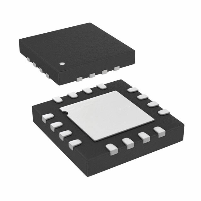
■ Available in a 16-pin (3mm × 3mm) MLF® package
APPLICATIONS
■ Data communication systems
■ Serial OC-192, OC-192+FEC data-to-clock
realignment
■ Parallel 10Gbps for OC768
■ All SONET OC-3 — OC-768 applications
■ All Fibre Channel applications
■ All GigE applications
FUNCTIONAL BLOCK DIAGRAM
TYPICAL APPLICATION
DATA
SY58052U
50Ω
VTD
50Ω
Data from
Backplane
(Uncertain timing)
DATA
/DATA
/DATA
Q
Q
CLK
/Q
/Q
50Ω
CLK
50Ω
/CLK
DATA
Q
Clock from Backplane
Retimed
Data
CLK
VTCLK
R
/CLK
DATA IN
CLK
/RESET
Q OUT
(Retimed)
AnyGate and Precision Edge are registered trademarks of Micrel, Inc.
MicroLeadFrame and MLF are registered trademarks of Amkor Technology, Inc.
M9999-082010
hbwhelp@micrel.com or (408) 955-1690
Rev.: D
1
Amendment: /0
Issue Date: August 2010
�Precision Edge®
SY58052U
Micrel, Inc.
GND
VCC
16
GND
VTCLK
PACKAGE/ORDERING INFORMATION
15
14
13
Ordering Information(1)
Part Number
Package
Type
Operating
Range
Package
Marking
Lead
Finish
SY58052UMI
MLF-16
Industrial
052U
Sn-Pb
GND
SY58052UMITR(2)
MLF-16
Industrial
052U
Sn-Pb
DATA
3
10
GND
SY58052UMG(3)
MLF-16
Industrial
/DATA
4
9
052U with
Pb-Free bar-line indicator
Pb-Free
NiPdAu
SY58052UMGTR(2, 3)
MLF-16
Industrial
052U with
Pb-Free bar-line indicator
Pb-Free
NiPdAu
5
6
7
8
VCC
Q
11
GND
12
2
/RESET
1
VTDATA
CLK
/CLK
/Q
16-Pin MLF® (MLF-16)
Notes:
1. Contact factory for die availability. Dice are guaranteed at TA = 25°C, DC electricals only.
2. Tape and Reel.
3. Pb-Free package recommended for new designs.
PIN DESCRIPTION
Pin Number
Pin Name
Pin Function
1, 2
CLK, /CLK
Differential Input: This input pair is the clock signal that re-times the data signal at DATA, /DATA.
Each pin of this pair internally terminates to the VTCLK pin to 50Ω. Note that this input will
default to an indeterminate state if left open. See “Input Interface Applications” section.
3, 4
DATA, /DATA
Differential Input: This input pair is the signal to be synchronized by the CLK, /CLK signal. Each
pin of this pair internally terminates to the VTD pin to 50Ω. Note that this input will default to an
indeterminate state if left open. See “Input Interface Applications” section.
5
VTData
Input Termination Center-Tap: Each of the two inputs, DATA, /DATA terminates to this pin. The
VTData pin provides a center-tap to a termination network for maximum interface flexibility.
See “Input Interface Applications” section.
6
/RESET
TTL/CMOS-Compatible Input: The /RESET input asynchronously forces the Q output to a logic
“0” state whenever it is active low. Possible state changes due to rising edges on CLK, /CLK are
ignored until /RESET goes inactive high.
7, 10, 11, 14, 15
GND
(Exposed Pad)
8, 13
VCC
Positive Power Supply. Bypass with 0.1µF0.01µF low ESR capacitors.
12, 9
Q, /Q
Differential Output: This CML output pair is the output of the flip-flop. The Data input is
transferred to the Q output at the rising edge of CLK (falling edge of /CLK). See “Input Interface
Applications” section.
16
VTCLK
Ground. Exposed pad must be connected to the same potential as the GND pin.
Input Termination Center-Tap: Each of the two inputs, CLK, /CLK terminates to this pin. The
VTCLK pin provides a center-tap to a termination network for maximum interface flexibility.
See “Input Interface Applications” section.
TRUTH TABLES
DATA
/DATA
CLK
/CLK
/RESET
Q
/Q
X
X
X
X
0
0
1
X
X
0
1
1
QN–1
/QN–1
X
X
1
0
1
QN–1
/QN–1
0
1
1
0
1
1
0
1
1
0
M9999-082010
hbwhelp@micrel.com or (408) 955-1690
2
�Precision Edge®
SY58052U
Micrel, Inc.
Absolute Maximum Ratings(1)
Operating Ratings(2)
Supply Voltage (VCC) .................................. –0.5V to +4.0V
Input Voltage (VIN) ......................................... –0.5V to VCC
CML Output Voltage (VOUT) ......... VCC –1.0V to VCC +5.0V
Termination Current(3)
Source or Sink Current on VTD, VCLK ....................... ±60mA
Input Current
Source or Sink Current on D, /D, CLK, /CLK ....... ±30mA
Lead Temperature (soldering, 20 sec.) ................... +260°C
Storage Temperature (TS) ....................... –65°C to +150°C
Supply Voltage (VCC) .......................... +2.375V to +2.625V
............................................................ +3.0V to +3.6V
Ambient Temperature (TA) ......................... –40°C to +85°C
Package Thermal Resistance(4)
MLF® (θJA)
Still-Air ............................................................. 61°C/W
MLF® (ψJB)
Junction-to-Board ............................................ 38°C/W
DC ELECTRICAL CHARACTERISTICS(5)
TA = –40°C to +85°C, unless otherwise noted.
Symbol
Parameter
Condition
VCC
Power Supply
ICC
Power Supply Current
RIN
Differential Input Resistance
(D, /D or CLK, /CLK)
VIH
Input HIGH Voltage
(D, /D or CLK, /CLK)
Note 6
VIL
Input LOW Voltage
(D, /D or CLK, /CLK)
VIN
Min
Typ
Max
Units
2.625
3.6
V
V
60
92
mA
100
120
Ω
1.2
VCC
V
Note 6
0
VIH–0.1
V
Input Voltage Swing
(D, /D or CLK, /CLK)
Note 6
100
mV
VDIFF_IN
Differential Input Voltage Swing
|D, /D| or |CLK, /CLK|
Note 6
See Figure 2a.
200
mV
|IIN|
Input Current
(IN, /IN)
Note 6
See Figure 2b.
2.375
3.0
No load, max. VCC.
80
21
mA
Notes:
1. Permanent device damage may occur if the ratings in the “Absolute Maximum Ratings” section are exceeded. This is a stress rating only and
functional operation is not implied for conditions other than those detailed in the operational sections of this data sheet. Exposure to absolute
maximum ratings conditions for extended periods may affect device reliability.
2. The data sheet limits are not guaranteed if the device is operated beyond the operating ratings.
3. Due to the limited drive capability use for input of the same package only.
4. Package thermal resistance assumes exposed pad is soldered (or equivalent) to the device’s most negative potential on the PCB. ψJB uses 4-layer
θJA in still-air, unless otherwise stated.
5. The circuit is designed to meet the DC specifications shown in the above table after thermal equilibrium has been established.
6. Due to the internal termination (see “ Input Structures” section) the input current depends on the applied voltages at D, /D and VTD inputs, the CLK,
/CLK and VTCLK inputs or the S, /S and VTS inputs. Do not apply a combination of voltages that causes the input current to exceed the maximum
limit!
M9999-082010
hbwhelp@micrel.com or (408) 955-1690
3
�Precision Edge®
SY58052U
Micrel, Inc.
LVTTL/CMOS DC ELECTRICAL CHARACTERISTICS(7)
VCC = 2.5V ±5% or 3.3V ±10%; TA = –40°C to +85°C; unless otherwise noted.
Symbol
Parameter
VIH
Input HIGH Voltage
VIL
Input LOW Voltage
IIH
Input HIGH Current
IIL
Input LOW Current
Condition
Min
Typ
Max
2.0
Units
V
–125
0.8
mV
20
µA
–300
µA
CML OUTPUTS DC ELECTRICAL CHARACTERISTICS(7)
VCC = 2.5V ±5% or 3.3V ±10%; RL = 100Ω across output pair or equivalent; TA = –40°C to +85°C; unless otherwise noted.
Symbol
Parameter
Condition
Min
VOH
Output HIGH Voltage Q, /Q
VOUT
Output Voltage Swing Q, /Q
See Figure 2a.
325
VDIFF_OUT
Differential Output Voltage Swing
Q, /Q
See Figure 2b.
ROUT
Output Source Impedance
Q, /Q
Typ
Max
Units
VCC
V
400
550
mV
650
800
1000
mV
40
50
60
Ω
VCC–0.020
AC ELECTRICAL CHARACTERISTICS(8)
VCC = 2.5V ±5% or 3.3V ±10%; RL = 100Ω across output pair or equivalent; TA = –40°C to +85°C; unless otherwise noted.
Symbol
Parameter
fMAX
Maximum Operating Frequency
tpd
Propagation Delay
tRESET
Propagation Delay
(RESET-to-Q)
tS
Set-Up Time
20
ps
tH
Hold Time
20
ps
tRR
Reset Recovery Time
500
ps
tJITTER
Random Jitter (RJ)
Note 9
Deterministic Jitter (DJ)
Note 10
tr, tf
Condition
Min
Typ
Max
10.7
(CLK-to-Q)
GHz
70
VTH = VCC/2
10–12
Total Jitter (TJ)
10GHz Clock, 1×
BER, Note 11
10GHz Data, 1× 10–12 BER, Note 11
Rise/Fall Times (20% to 80%)
At full output swing.
20
Units
30
190
ps
600
ps
1
psRMS
10
psPP
10
14
psPP
psPP
60
ps
Notes:
7.
The circuit is designed to meet the DC specifications shown in the above table after thermal equilibrium has been established.
8.
Measured with 100mV input swing. See “Timing Diagrams” section for definition of parameters. High-frequency AC-parameters are guaranteed by
design and characterization.
9.
RJ is measured with a K28.7 comma detect character pattern, measured at 10.7Gbps and 2.5Gbps.
10. DJ is measured at 10.7Gbps and 2.5Gbps, with both K28.5 and 223–1 PRBS pattern
11. Total jitter definition: with an ideal clock input frequency of ≤ fMAX, no more than one output edge in 1012 output edges will deviate by more than
the specified peak-to-peak jitter value.
M9999-082010
hbwhelp@micrel.com or (408) 955-1690
4
�Precision Edge®
SY58052U
Micrel, Inc.
TYPICAL OPERATING CHARACTERISTICS
VCC = 3.3V, GND = 0V, CLK = 400mV, D = 400mV, TA = 25°C.
622Mbps Output
1.25Gbps Output
Output Swing
(50mV/div.)
PRBS 223—1
Output Swing
(50mV/div.)
PRBS 223—1
TIME (500ps/div.)
TIME (200ps/div.)
2.5Gbps Output
5Gbps Output
Output Swing
(50mV/div.)
PRBS 223—1
Output Swing
(50mV/div.)
PRBS 223—1
TIME (100ps/div.)
TIME (50ps/div.)
7Gbps Output
10.7Gbps Output
Output Swing
(50mV/div.)
PRBS 223—1
Output Swing
(50mV/div.)
PRBS 223—1
TIME (20ps/div.)
Output Amplitude
vs. Data Rate
IN to Q Propagation Delay
vs. Temperature
OUTPUT AMPLITUDE (mV)
PROPAGATION DELAY (ps)
140
TIME (20ps/div.)
135
130
CML (200mV Swing)
125
120
115
110
LVDS (400mV Swing)
PECL (800mV Swing)
105
100
-60 -40 -20 0 20 40 60 80 100
TEMPERATURE (°C) (Forced Air)
M9999-082010
hbwhelp@micrel.com or (408) 955-1690
5
420
400
380
360
340
320
300
280
260
240
220
200
0
2
4
6
8
10
DATA RATE (Gbps)
12
�Precision Edge®
SY58052U
Micrel, Inc.
TIMING DIAGRAM
CLK
tH
50%
50%
DATA
tS
tRR
/RESET
50%
50%
Q
tpd
tpd
INPUT AND OUTPUT STAGE INTERNAL TERMINATION
VCC
VCC
VCC
50Ω
50Ω
/Q
Q
R
CLK, DATA
/RESET
50Ω
VTCLK, VTD
R
50Ω
/CLK, /DATA
Figure 1c. Simplified
Differential Output Stage
Figure 1b. Simplified
TTL/CMOS Input
Figure 1a. Simplified
Differential Input Stage
OPERATING CHARACTERISTICS
VDIFF_IN, VDIFF_OUT
800mV (typical)
VIN, VOUT
400mV
(typical)
Figure 2a. Single-Ended Swing
Figure 2b. Differential Swing
Definition of Single-Ended and Differential Swings
M9999-082010
hbwhelp@micrel.com or (408) 955-1690
6
�Precision Edge®
SY58052U
Micrel, Inc.
INPUT INTERFACE APPLICATIONS
VCC
VCC
VCC
D
D, CLK
1kΩ
D, CLK
LVDS
/D
CML
/D, /CLK
SY58052U
/D, /CLK
SY58052U
GND
SY58052U
GND
NC
GND
VT
NC
NC
VT
VT
Input HIGH level shown.
Figure 3b. LVDS
Interface (DC-Coupled)
Figure 3a. Static Input Level
Figure 3c. CML
Interface (DC-Coupled)
Option: VT may be connected to VCC.
VCC
VCC
VCC
0.1µF
0.1µF
D, CLK
CML
/D, /CLK
VCC
/D, /CLK
/D, /CLK
VCC
GND
R1
LVPECL
LVPECL
SY58052U
GND
0.1µF
D, CLK
D, CLK
SY58052U
0.1µF
VT
R1 = 1kΩ, R2 = 1.4kΩ.
Figure 3d. CML
Interface (AC-Coupled)
RPD
VCC
SY58052U
GND
0.1µF
VT
Rb
R2
RPD
R1
VT
R2
GND
Rb = 50Ω.
GND
Figure 3e. LVPECL
Interface (DC-Coupled)
For 3.3V, RPD = 100Ω.
R1 = 1kΩ, R2 = 1.4kΩ.
For 2.5V, RPD = 50Ω.
R1 = 1kΩ, R2 = 1.4kΩ.
Figure 3f. LVPECL
Interface (AC-Coupled)
RELATED PRODUCT AND SUPPORT DOCUMENTATION
Part Number
Function
Data Sheet Link
SY58016L
3.3V 10Gbps Differential CML Line Driver/
Receiver with Internal Termination
www.micrel.com/product-info/products/sy58016l.shtml
SY58051U
10.7Gbps AnyGate® with Internal Input and
Output Termination
www.micrel.com/product-info/products/sy58051u.shtml
MLF® Application Note
www.amkor.com/products/notes_papers/MLF_AppNote_0902.pdf
New Products and Applications
www.micrel.com/product-info/products/solutions.shtml
HBW Solutions
M9999-082010
hbwhelp@micrel.com or (408) 955-1690
7
�Precision Edge®
SY58052U
Micrel, Inc.
16-PIN MicroLeadFrame® (MLF-16)
Package
EP- Exposed Pad
Die
CompSide Island
Heat Dissipation
Heat Dissipation
VEE
Heavy Copper Plane
VEE
Heavy Copper Plane
PCB Thermal Consideration for 16-Pin MLF® Package
(Always solder, or equivalent, the exposed pad to the PCB)
Package Notes:
1. Package meets Level 2 qualification.
2. All parts dry-packaged before shipment.
3. Exposed pads must be soldered to a ground for proper thermal management.
MICREL, INC. 2180 FORTUNE DRIVE SAN JOSE, CA 95131
TEL
+ 1 (408) 944-0800
FAX
+ 1 (408) 474-1000
WEB
USA
http://www.micrel.com
The information furnished by Micrel in this data sheet is believed to be accurate and reliable. However, no responsibility is assumed by Micrel for its use.
Micrel reserves the right to change circuitry and specifications at any time without notification to the customer.
Micrel Products are not designed or authorized for use as components in life support appliances, devices or systems where malfunction of a product can
reasonably be expected to result in personal injury. Life support devices or systems are devices or systems that (a) are intended for surgical implant into
the body or (b) support or sustain life, and whose failure to perform can be reasonably expected to result in a significant injury to the user. A Purchaser’s
use or sale of Micrel Products for use in life support appliances, devices or systems is at Purchaser’s own risk and Purchaser agrees to fully indemnify
Micrel for any damages resulting from such use or sale.
© 2005 Micrel, Incorporated.
M9999-082010
hbwhelp@micrel.com or (408) 955-1690
8
�


 工商网监
湘ICP备2023018690号
工商网监
湘ICP备2023018690号
